


Flip Chips |
|

|
Flip Chip describes the method of electrically connecting the die to the package carrier. The package carrier, either substrate or leadframe, then provides the connection from the die to the exterior of the package. The interconnection between die and carrier in flip chip packaging is made through a conductive bump that is placed directly on the die surface. The bumped die is then flipped over and placed face down, with the bumps connecting to the carrier. After the die is soldered, underfill is applied between the die and the substrate, around the solder bumps. The underfill is designed to contract the stress in the solder joints caused by the difference in thermal expansion between the silicon die and carrier. |
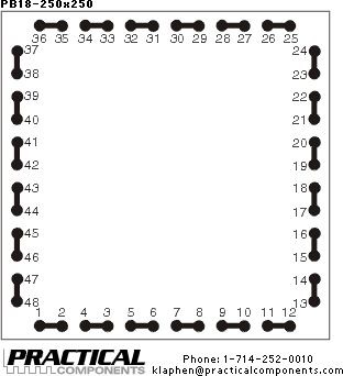
| Part Number | PB18- 250 x 250 |
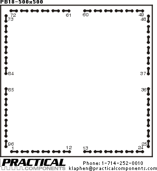
PB18- 500 x 500 |
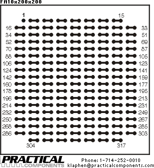
FA10- 200 x 200 |
PB08- 200 x 200 PB08- 400 x 400 |
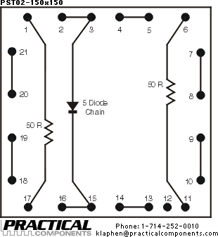
PST02- 150 x 150 |
|
| Drawings | See Drawing | See Drawing | See Drawing | See Drawing | See Drawing | |
| Die Size | 250 x 250 mils | 500 x 500 mils | 200 x 200 mils | 200 x 200 mils 400 x 400 mils |
150 x 150 mils | |
| Bump Pitch | 457 µm, 18 mil | 457 µm, 18 mil | 254 µm, 10 mil | 203 µm, 8 mil | 457 µm, 18 mil | |
| Passivation Via | 102 µm | 102 µm | 80 µm | 73 µm | 102 µm | |
| UBM Diameter | 152 µm | 152 µm | 102 µm | 95 µm | 152 µm | |
| Bump Height | 140 µm | 140 µm | 110 µm | 98 µm | 130 µm | |
| Bump Diameter | 190 µm | 190 µm | 135 µm | 120 µm | 160 µm | |
| No. of Bumps | 48 | 96 | 317 | 88 | 21 | |
| Max. Bump Diagonal | 7.7 mm | 16.5 mm | 7.9 mm | — | — | |
| Die Metal | Pad Size | 193 x 193 µm | 193 x 193 µm | 127 x 127 µm | 115 x 115 µm | 165 x 165 µm |
| Thickness | 12 kA | 12 kA | 12 kA | 12 kA | 40 kA | |
| Type | 98/1/1 Al/Cu/Si | 98/1/1 Al/Cu/Si | 98/1/1 Al/Cu/Si | 98/1/1 Al/Cu/Si | 98/1/1 Al/Cu/Si | |
| Packaging | ||||||
| Uncut Wafer* | 5" Wafer 250 x 250 mils (236 Die) |
5" Wafer 500 x 500 mils (46 Die) |
5" Wafer 200 x 200 mils (375 Die) |
5" Wafer 200 x 200 mils (375 Die) 400 x 400 mils (87 Die) |
5" Wafer 150 x 150 mils (694 Die) |
|
| Tray | Sawed 5" Wafer 25 per tray 2" sq Waffle Pack |
Sawed 5" Wafer 9 per tray 2" sq Waffle Pack |
Sawed 5" Wafer 36 per tray 200 x 200 Waffle Pack |
Sawed 5" Wafer 36 per tray 200 x 200 9 per tray 400 x 400 Waffle Pack |
Sawed 5" Wafer 25 per tray 2" sq Waffle Pack |
|
| Tape and Reel | Call For Availability | Call For Availability | Call For Availability | Call For Availability | Call For Availability | |
- * Die count represents expected yield per wafer.
- All die is packaged in waffle pack trays unless otherwise specified.
- All test wafers are currently 5" diameter and are 0.635mm thick. Passivation is one-micron thick plasma nitride with round via openings.
- The potential multiple is the number of die repeats on the wafer. With the wafer orientated flat down, a right hand coordinate system applies.
- Die size is from scribe line to center-to-center. Scribe width is 0.05mm passivated. Each bump is electrically connected to one other bump and isolated from all others to facilitate electrical test.
- Bump pitch is defined as center-to-center distance between passivation openings.
- Bump height is defined as silicon surface to the top of the bump.
- Bump diameter is defined as the maximum diameter.
- UBM = Under Bump Metallurgy
- Lead-free parts are available.
About Lead-Free Flip Chips
Flip Chips are used in evaluating assembly techniques, board continuity, temperature cycle life test evaluation, underfill processes and other generic Flip Chip evaluations. When using Lead-Free Flip Chips, consideration needs to be given to the appropriate flux, underfill, temperature profile, and pad finish for the assembly. Many companies are developing and qualifying alternative pad finishes such as immersion Sn. Lead-Free Flip Chips address the need for environmentally conscious assemblies as well as Alpha particle tolerant packaging.
Lead-Free Die
- All Flip Chips are available Lead-Free with Alloy LF2 composition 95.5% Sn /3.5% Ag /1.0% Cu.
- When ordering Lead-Free Flip Chips, add “LF2” at end of part number.
- LF2 was introduced by FCT (the acronym is Lead-Free #2). Please call for more details.
Quartz Die
- When ordering Quartz chips, add “Q” at end of part number. For Quartz Lead-Free add “QLF2”.
- Quartz allows customers to observe underfill processes. Please call for more details.
- All Flip Chips are available in “Quartz” with eutectic solder bumps or Lead-Free.